
config of a semiconductor wafer back grinding equipment manufacturer Grasping strong production capability, advanced research strength and excellent service, Shanghai config of a semiconductor wafer back grinding equipment supplier create the value and bring values to all of customers.
 WhatsApp)
Apr 28, 2017· Our "RAD-3510F/12" is a system that laminates tapes for protecting the circuit sides of wafers during back grinding or thinning process of wafers after circuits are formed on them. It reduces the risk of damage during in-line wafer transport and is capable of handling both wafers with bumps and ultra-thin wafers.
Sep 02, 2017· Wafer backgrinding is a semiconductor device fabrication step during which wafer thickness is reduced to allow for stacking and high density packaging of integrated circuits (IC).
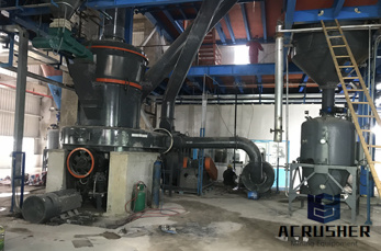
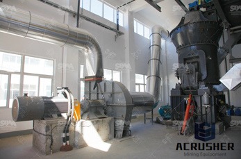
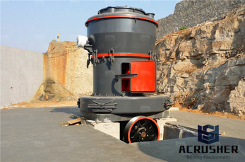
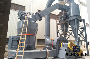
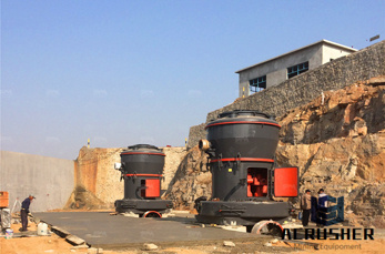
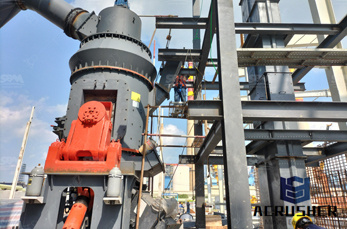
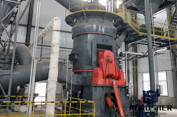
It is the page for our semiconductor manufacturing equipment. It introduces such as wafer manufacturing system, SMP, Wafer probing machine, Polish grinder, Wafer dicing machine, High-rigidity grinder and Blade for precision cutting.
This paper addresses an important aspect of silicon wafer fine grinding: machine design. For any commercially available wafer grinders, spindle angle adjustments based on the wafer shape ground is almost inevitable in order to achieve flat wafers.
Wafers that flow through SVM's advanced reclaim programs successfully characterize 45nm particles and site flatness at 0.13μm. By utilizing state of the art reclaim equipment, SVM is able to reclaim wafers with a minimal amount of silicon removal (as low as 3μm), as well as the highest yields in the industry. SVM Wafer Reclaim Capabilities:
Thinning by grinding. Back grinding is the conventional method for reducing wafers from their original thickness to a diminished thickness suitable for final packaging of die after dicing. Grinding is fast and produces low variation and good surface finishes.
Syagrus Systems is a leading service provider specializing in post-fab processes for semiconductor and electronic component manufacturers worldwide. We have become a leader in semiconductor and silicon wafer back end processing by listening to our customers' needs, working with them to create the solution and then exceeding their expectations.
Leading-edge Tape × Equipment solution created with semiconductor-related products 'Adwill.' Wafer surface protection tapes and peeling tapes for the back grinding Process. ... Fully protects the wafer surface during back grinding and prevents wafer surface contamination from infiltration of grinding fluid and/or debris. 2. There is virtually ...
Koyo Machinery is a world leader in the development and manufacturing of custom Centerless, Surface and Specialty Grinders. We repair and install specialty grinders for a variety of industries including Automotive, Aerospace, Bearing, Construction, Energy and Medical
Wafer backgrinding is a semiconductor device fabrication step during which wafer thickness is reduced to allow stacking and high-density packaging of integrated circuits (IC).. ICs are produced on semiconductor wafers that undergo a multitude of processing steps. The silicon wafers predominantly used today have diameters of 200 and 300 mm. They are roughly 750 μm thick to ensure a minimum .
Back grinding is a process that removes silicon from the back surface of a wafer. Silicon Valley Microelectronics provides grinding on our own substrates or on customer supplied wafers. We process bare and device patterned wafers with high yield and offer wafer thinning to customer specifications. SVM Wafer Back Grinding Capabilities:
In addition, in April 2017, LINTEC launched Back Grinding Tape Laminator RAD-3520F/12 that protects circuit surface of the wafer during the back grinding and thinning process of the semiconductor ...
Jan 29, 2020· Jan 29, 2020 (Global QYResearch via COMTEX) -- A new research report titled "Global Semiconductor Wafer Polishing and Grinding Equipments .
Wafer Back Grinding Tapes NON-SILICONE, NON-EVA BASED COMPRESSIBLE BACKGRINDING AND THINNING TEMPORARY BONDING ADHESIVE TAPES FOR BUMPED WAFERS AND SUBSTRATES WITH UP TO 250 MICRON BUMP HEIGHTS: The configuration of the temporary bonding adhesive tapes are engineered for high reliability for wafers and substrates with extensive .
Feb 05, 2016· A 300 mm wafer mounted on a standard film frame is spin coated using multiple chemistries under fully automatic control. ... Wafer Sawing Machine - Duration: ... Semiconductor Fabrication Basics ...
・Air back presser system and scanning polish remove the grinding damage evenly. ・As option, Coin stack unit is available for thin wafer. ・It can be used as a stand alone machine not only in-line system with grinder, which satisfy the various type low volume products request.
Effect of Wafer Back Grinding on the Mechanical Behavior of Multilayered Low-k for 3D-Stack Packaging Applications V. N. Sekhar*, Lu Shen#, Aditya Kumar, T. C. Chai, Lee Wen Sheng Vincent, Wang Xin Lin Sandy, Xiaowu Zhang, C. S. Premchandran, V. Kripesh, John H. Lau
Oct 01, 2019· In addition, in April 2017, LINTEC launched Back Grinding Tape Laminator RAD-3520F/12 that protects circuit surface of the wafer during the back grinding and thinning process of the semiconductor ...
Grinding Machines for Semiconductor Wafers Koyo Machine Industries developed several types of grinding machines, used in the semiconductor industry for silicon wafer manufacturing and IC production. Vertical and horizontal spindle systems are used in combination with special designed diamond grinding wheels, that cut just at the edge of the ...
In the context of manufacturing integrated circuits, wafer dicing is the process by which die are separated from a wafer of semiconductor following the processing of the wafer. The dicing process can involve scribing and breaking, mechanical sawing (normally with a machine .
GDSI, Grinding and Dicing Services complete resource for Silicon Wafers Processing includes Probing, Bumping, Grinding, Polishing in San Jose, California.
Dec 02, 2014· 🔴 Sleep Music 24/7, Sleep Meditation, Calm Music, Insomnia, Sleep Therapy, Spa, Study, Relax, Sleep Yellow Brick Cinema - Relaxing Music 3,077 watching Live now
At Nitto, various products meeting the advanced needs of numerous processes during electronic device production are created, based on a wealth of experience and knowledge gained in the field of electric and electronic materials.
Wafer Backgrind Wafer Backgrind is the process of grinding the backside of the wafer to the correct wafer thickness prior to assembly. It is also referred to as 'wafer thinning.' Wafer backgrinding has not always been necessary, but the drive to make packages thinner and thinner has made it indispensable.
WhatsApp)